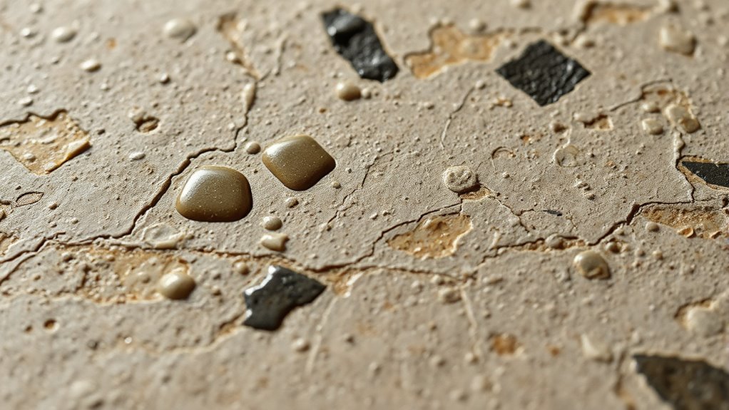
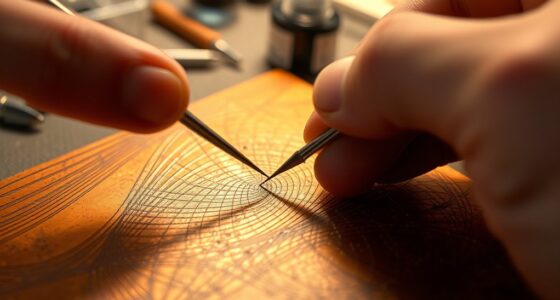
Planographic lithography is a technique that uses a flat surface, like a stone or silicon wafer, to create detailed patterns through chemical processes. You coat the surface with a light-sensitive material called photoresist and expose it to UV light through a mask. The chemicals change in exposed areas, allowing you to wash away certain parts and form precise designs. If you keep exploring, you’ll discover how this method drives modern microelectronics and technology advancements.
Key Takeaways
- Lithography is a planographic technique where images are created on a flat surface, with the design and non-design areas sharing the same level.
- It relies on the immiscibility of oil and water, using chemical principles to differentiate areas for printing or patterning.
- Modern lithography involves coating surfaces with photoresist, exposing it to light through masks, and developing the pattern chemically.
- In microfabrication, lithography enables high-precision pattern transfer for manufacturing microelectronic components.
- Evolving from traditional art to industrial processes, lithography plays a critical role in producing high-resolution, intricate patterns on surfaces.

Have you ever wondered how tiny circuits are etched onto computer chips? The answer lies in a fascinating technique called lithography, which uses a chemical process to transfer intricate patterns onto surfaces. But before it became the cornerstone of modern electronics, lithography underwent a significant historical development that shaped its present form. Originally, lithography was invented in the late 18th century as a printing method, relying on the principle that oil and water don’t mix. This process was used for creating images and text on paper, utilizing a flat stone surface—hence the name “lithography,” meaning “stone writing” in Greek. Over time, scientists adapted this concept for manufacturing, discovering that the flat surface could carry patterns with high precision through a chemical process. This shift marked the beginning of its evolution from art printing to a crucial tool in microfabrication.
The modern form of lithography involves a chemical process that uses a photosensitive substance called a photoresist. You start by coating a flat surface—often a silicon wafer—with this light-sensitive material. Then, you expose the coated surface to ultraviolet (UV) light through a patterned mask. The areas of the photoresist exposed to light undergo a chemical change, making them either more or less soluble depending on whether you’re using a positive or negative photoresist. When you develop the pattern, the exposed or unexposed regions are washed away, revealing the underlying surface in specific shapes. This chemical process allows you to create incredibly detailed patterns necessary for microelectronics. The development of photolithography was a pivotal moment, enabling the production of microchips with nanometer precision.
The historical development of lithography’s adaptation for semiconductor manufacturing was driven by the need for higher resolution and precision. Early techniques used simple contact printing, but as circuits became more complex, scientists needed more refined methods. That’s when the introduction of photolithography, with its reliance on chemical reactions and light exposure, revolutionized the industry. This advancement enabled the production of smaller, faster, and more efficient chips by allowing patterning at nanometer scales. Today, lithography continues to evolve, incorporating new chemical processes and materials to keep pace with the demand for miniaturization. Its development from a simple printing technique to a sophisticated manufacturing process highlights the importance of chemical processes and innovation in technology’s progress, shaping the tiny yet powerful devices that run our digital world.
Top picks for "planographic techniqu lithography"
Open Amazon search results for this keyword.
As an affiliate, we earn on qualifying purchases.
Frequently Asked Questions
What Are the Environmental Impacts of Lithography?
You should be aware that lithography can have significant environmental impacts, mainly through chemical waste and energy consumption. The process uses chemicals that, if not properly managed, can pollute water and soil. Additionally, it requires substantial energy, contributing to carbon emissions. By adopting eco-friendly practices and proper waste disposal, you can minimize these effects and make lithography more sustainable for the environment.
How Does Digital Lithography Differ From Traditional Methods?
Digital lithography revolutionizes the process by using digital imaging technology instead of traditional chemical methods, making pattern transfer almost instantaneous. You get ultra-precise designs without messy plates or chemicals, drastically reducing environmental impact. With digital techniques, you can modify patterns on the fly, allowing for rapid prototyping and customization. This shift not only speeds up production but also eliminates many hazards associated with traditional lithography, making it a cleaner, greener choice.
What Are the Limitations of Lithography in Modern Manufacturing?
You face limitations in lithography due to scaling challenges and resolution limits. As devices shrink, maintaining precision becomes harder, leading to increased defects and reduced yields. Traditional lithography struggles with achieving ultra-fine features needed for advanced electronics, forcing you to explore newer methods like EUV. These constraints hinder continued miniaturization, making it difficult to keep pace with the demands of modern, high-performance manufacturing.
How Is Lithography Used in Semiconductor Fabrication?
You harness lithography in semiconductor fabrication to achieve unparalleled precision in wafer patterning. Through photolithography processes, you project intricate circuit designs onto silicon wafers, enabling you to create microscopic features that define modern electronics. This technique allows you to produce billions of transistors on a single chip, pushing the boundaries of miniaturization and performance, revolutionizing the way you develop faster, smaller, and more powerful semiconductors.
What Are Emerging Trends in Lithographic Technology?
You’ll see emerging trends like nanolithography advancements, enabling you to create smaller, more precise features in chips, boosting performance. Eco-friendly lithography gains momentum, helping you reduce environmental impact through less hazardous chemicals and energy-efficient processes. These innovations allow you to push the boundaries of semiconductor fabrication, making your production more sustainable and capable of meeting the demands for higher density and faster devices in the future.
Conclusion
Now that you understand how lithography works, you might think you’ve uncovered all its secrets. But beneath the surface, countless innovations and hidden techniques await discovery. Will you explore further, or let this be just the beginning of your journey into printmaking’s mysterious world? The truth is, every detail you uncover could lead to something extraordinary—something you never saw coming. So, are you ready to dive deeper and reveal even more of lithography’s secrets?


